Some
Results
— Highest
CVD diamond
Model AX5000/AX5200
Model AX5250/AX5400
Model AX6550/6560
Model AX6600 |
|
|
| From
Model AX5000/5200
The AX5000 /
AX5200 incorporate process development for the growth of high quality
CVD diamond films for application in electronics, optics, thermal
management, and tools. The AX5000 deposits CVD diamond on 2-in diameter
substrates with good thickness uniformity substrates up to 4-in
diameter can be accommodated.
 |
 |
| Raman
spectrum of a CVD diamond films |
SEM
of a diamond film |
| |
Diamond
membrane approximately 2 mm thick
(Membrane courtesy of Dr. H.dishmann, BP America, Inc.) |
|
|
| From
Model
AX5250/AX5400
The AX5400/AX5250 incorporate process development for the growth
of highest quality CVD diamond films at very high growth rates.
Uniform, free standing diamond materials for advanced applications
are obtained.
|
 |
| SEM
of a thick diamond film |
Raman
spectrum of a CVD diamond films |
| |
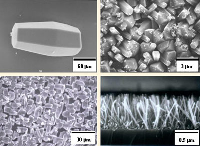
Examples
of thick CVD Diamond films suitable for heat sink applications
(the larger wafer is 2 in. diameter) |
|
|
| High
power density microwave plasmas |
Diamond
deposition at high power densities has yielded more than one-of-magnitude
improvement of the linear growth rates previously possible in similar
reactors at lower power densities. In this new system, diamond deposition
rates of up to 60 mg/hour have been demonstrated. Linear growth
rates of 15micro meter/hour near the center of the sample have been
measured. Figure 1 shows a cross-section of a diamond film grown
at such rates. Note the columnar structure characteristic of high
growth rate depositions. Figure 2 shows a top view of the films.
Nicely faced material is obtained. At these high rates, thick free-standing
films are possible within a few hours of deposition.
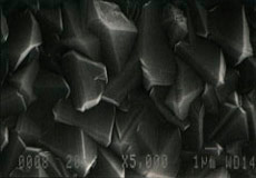
Figure 3 shows
preferential alignment of the crystals along the [100] direction
which is obtained under some deposition conditions. Preferential
alignment of the facets can have applications for these CVD films
in active electronics.
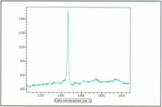
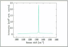
The thermal
conductivity of diamond films samples grown at rates near 3micro
meter m/hour was measured using two different techniques. The measurements
yielded values of the thermal conductivity in the 10 to 20 W/cm-K
range. This high thermal conductivity value makes such films ideal
for heat sink applications. As an example, the Raman spectrum for
one of these films is shown in Figure 4. The FWHM of the diamond
line near 1332cm-1 was measured at 6cm-1. This value is close to
the width for natural diamond (approximately 2 cm-1). Such narrow
width lines are characteristic of high quality CVD diamond.
|
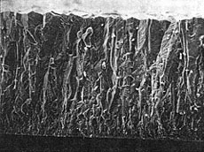
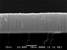
Figure 1. SEM
cross-section of diamond film
grown at 15micro meter per hour.
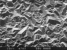
Figure 2. Surface of diamond film shown in
Figure 1.
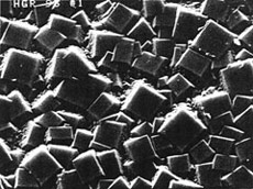
Figure 3. SEM of diamond film grown at 5micro meter per hour, showing
preferential [100] alignment.
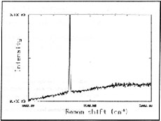
Figure 4. Raman
spectrum of typical diamond film
|
|
| From
Model AX6550/6560
AX6550/AX6560
are the reactors in a series that incorporates former ASTeX newest
development in microwave reactor technology. The AX6550/AX6560 enable
the user sufficient production capacity to capture a significant
market share in the rapidly expanding thermal management and the
highly competitive tool markets.
|
Figure
1 shows silicon wafer in a 4-inch diameter loading platform.
The AX6550/AX6560 is designed to provide clear and easy access
to substrates, making loading and unloading a simple operation.This
design also allows the straightforward implementation of robotics
for loading operations.
|
Figure 1:
A 4-inch diameter silicon wafer on the AX 6550 substrate stage.
|
Figure
2 shows an example of a loading configuration for SPG422 inserts
over a 4 inch diameter loading area.
|
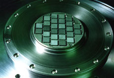
Figure 2:
SPG422 inserts in standard tool figure on AX 6560 substrate
stage. |
| The
AX6500 Series of reactors is designed to satisfy customer needs
in all application areas for thin and thick diamond films. Specialized
reactors are available or under development for each application
area, including thermal management, tool inserts, optics, and
electronics. |
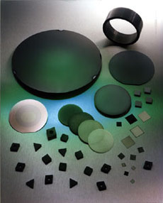
Figure 3:
Examples of thick diamond films suitable for thermal management
applications, as well as CVD diamond-coated wafers and tool
inserts. |
|
|
Model
AX6600
| The
AX6600 is the latest model designed to meet the scale-up needs
of large area coating of diamond.
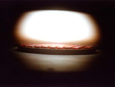
Photograph
shows the plasma and a typical batch of tool inserts during
processing in the AX6600.
|
 |
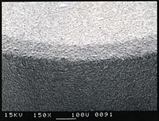
| SEM
photograph of an insert coated with CVD diamond in the AX6600
reactor the thickness of the coating is approximately is micrometer. |
 |
|
|
| Advanced
Materials
Seki microwave
plasma CVD systems are now routinely used to deposit aligned carbon
nanotubes (Figure 1), nanocrystalline diamond (Figure 2), and silicon
carbonitride materials (Figure 3).
| Figure
1. |
SEM
micrograph showing aligned carbon nanotubes grown by microwave
plasma assisted CVD (Courtesy of L. C. Chen, National Taiwan
University K. H. Chen, Academia Sinica) |
|
| Figure
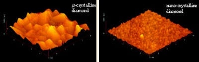
2. |
Example
of micro and nano-crystalline diamond films grown in AX5000
(Courtesy of T. Soga, Nagoya Institute of Technology) |
| |
|
| Figure
3. |
Silicon
Carbonitride (SixCyNx) crystals and aligned nano rods formed
using microwave plasma (Courtesy of L. C. Chen, National Taiwan
University K. H.Chen, Academia Sinica) |
| |
|
Top
of Page
|
| |